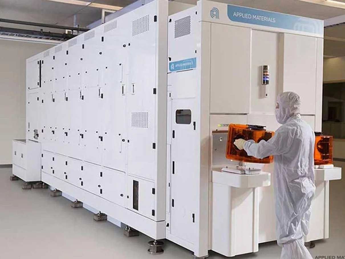
Applied Materials has agreed to increase its stake in Dutch semiconductor equipment manufacturer Besi from 9% to approximately 20%. Behind this investment lies a much larger industrial contest: the race to master the technologies that will connect processors, memory and other components powering the next generation of artificial intelligence. Europe retains critical technological expertise, but the growing involvement of American capital raises fundamental questions about industrial influence, strategic autonomy and the future distribution of value across the semiconductor industry.
An Investment That Goes Beyond Financial Ownership
On October 26, 2026, Applied Materials announced a transaction that could have lasting implications for the global semiconductor industry.
The American semiconductor equipment manufacturer entered into an agreement to increase its ownership of BE Semiconductor Industries, commonly known as Besi, to approximately 20%.
The Dutch company specializes in semiconductor assembly equipment, a segment whose strategic importance is increasing as the industry moves beyond the traditional pursuit of ever-smaller transistors.
The transaction builds on an initial investment made in April 2025, when Applied Materials acquired approximately 9% of Besi, becoming its largest shareholder.
Within eighteen months, the American group has therefore undertaken two successive steps to deepen its financial relationship with a European manufacturer operating in a critical area of advanced semiconductor production.
The October 26 agreement, however, does not constitute a majority acquisition.
Applied Materials has signed an accelerated share purchase agreement, with delivery of the additional shares subject to the expiration or termination of the waiting period applicable under the US Hart-Scott-Rodino Act.
The company has also stated that it does not currently intend to increase its ownership beyond approximately 20% or seek representation on Besi's board of directors.
Neither the acquisition price nor the exact number of additional shares has been publicly disclosed in the documents examined.
These distinctions matter.
Applied Materials is strengthening its economic position in Besi without acquiring legal control of the Dutch company.
Yet the industrial significance of the transaction may extend far beyond its financial structure.
Why Semiconductor Packaging Is Becoming a Strategic Technology
For decades, progress in computing was driven primarily by the miniaturization of transistors.
The ability to integrate more transistors onto a single silicon chip allowed manufacturers to increase computing power while gradually improving energy efficiency.
That process remains important, but it is encountering increasingly demanding physical, technological and economic constraints.
As semiconductor components become more complex, manufacturing costs rise and the performance improvements achievable through miniaturization alone become more difficult to obtain.
Artificial intelligence is accelerating this transformation.
Modern AI systems require enormous computing capacity, but they also depend on substantial memory resources and the continuous movement of data between different components.
Moving information within a computing system consumes energy and introduces delays that can constrain overall performance.
The industrial challenge is therefore no longer limited to producing faster transistors.
It increasingly involves determining how those transistors, processors and memory components are connected.
This is precisely where Besi occupies a strategic position.
The company develops equipment capable of assembling semiconductor components with extremely high precision.
These technologies help bring processors, memory and other electronic components closer together, improving the architecture of advanced computing systems.
The implications are substantial.
When data movement becomes a limiting factor, the quality and density of interconnections can determine a growing share of a system's performance.
Advanced packaging is therefore moving beyond its traditional role as a final manufacturing step.
It is becoming an essential element of semiconductor architecture itself.
Hybrid Bonding and the Next Generation of Computing
Among Besi's technologies, hybrid bonding occupies a particularly important position.
This process enables extremely fine, direct connections between semiconductor surfaces.
Compared with conventional assembly methods that rely on larger interconnections, hybrid bonding can increase connection density while reducing the distances electrical signals must travel.
The objective is to improve computing performance, energy efficiency and the physical integration of electronic components.
These advantages are particularly relevant to artificial intelligence.
AI accelerators must process growing volumes of information, while demand for memory capacity and bandwidth continues to expand.
Three-dimensional integration offers the possibility of constructing architectures in which different semiconductor components are stacked or positioned in close proximity.
Advanced bonding technologies become essential to manufacturing these systems.
This does not mean hybrid bonding will immediately replace existing assembly methods.
Its adoption depends on manufacturing yields, production costs, connection reliability and the ability of semiconductor manufacturers to deploy the technology at industrial scale.
Nevertheless, it is already changing how value is distributed across the semiconductor supply chain.
Companies capable of mastering critical integration processes can establish competitive advantages that do not depend exclusively on manufacturing the chips themselves.
They help determine which computing architectures can be built, how efficiently they operate and how economically they can be produced.
The strategic importance of semiconductor manufacturing is therefore expanding beyond transistor fabrication.
It increasingly includes the technologies required to connect individual components into functional computing systems.
A Partnership Built Over Six Years
The relationship between Applied Materials and Besi did not begin with the October 2026 investment.
Their industrial cooperation dates back to 2020, when the companies began collaborating on hybrid bonding technologies.
That relationship included the establishment of a hybrid bonding center of excellence in Singapore.
The industrial logic was clear.
Applied Materials possesses extensive expertise in semiconductor manufacturing equipment, materials engineering and production processes.
Besi specializes in the technologies required to assemble and integrate semiconductor components.
Combining these capabilities allows the companies to develop processes that must operate together, from surface preparation to the final bonding of components.
On October 1, 2026, the two groups announced an expansion of their strategic partnership.
Their cooperation now covers several areas, including three-dimensional integrated circuits, logic and memory integration, photonic applications, hybrid bonding and advanced thermocompression technologies.
The companies are also working on different packaging configurations, including chip-to-wafer and chip-to-chip integration, as well as technologies involving larger substrates.
The objective is to enable the industrial production of increasingly complex semiconductor systems.
The additional investment announced twenty-five days later therefore extends an established technological relationship.
It does not create the partnership.
It gives that partnership a stronger financial dimension.
A $5 Billion Innovation Ecosystem
The investment becomes even more significant when considered alongside Applied Materials' broader industrial strategy.
On October 12, 2026, the American company presented its EPIC Center, short for Equipment and Process Innovation and Commercialization, in Silicon Valley.
The initiative represents a planned investment of approximately $5 billion.
Its purpose is to bring semiconductor manufacturers, equipment suppliers, system designers and research teams closer together to accelerate the development and commercialization of new technologies.
Besi is among the innovation partners associated with the initiative.
The project illustrates a fundamental transformation in semiconductor manufacturing.
As electronic architectures become more complex, different stages of production must increasingly be developed in coordination.
The performance of a semiconductor component depends not only on its individual characteristics but also on its compatibility with materials, packaging technologies and interconnection processes used throughout the final system.
Industrial research centers are therefore becoming more than facilities dedicated to technological experimentation.
They are increasingly environments in which future relationships between suppliers, manufacturers and customers are established.
For Applied Materials, a larger stake in Besi may help consolidate cooperation within this ecosystem.
For Besi, access to extensive research capabilities and a global industrial network may facilitate the development and commercialization of advanced packaging solutions.
These complementarities do not guarantee commercial success.
They do, however, explain why financial investment and technological cooperation are becoming increasingly interconnected.
Demand Is Beginning to Translate Into Orders
Besi's recent financial performance provides additional context for Applied Materials' decision.
On October 22, 2026, four days before the investment announcement, the Dutch company reported quarterly orders of €342.6 million.
That represented an increase of approximately 17% from the previous quarter and 96% year over year.
Orders also exceeded analysts' expectations of approximately €298 million.
The difference amounted to nearly €45 million.
The increase came amid sustained demand for equipment supporting advanced computing infrastructure and artificial intelligence applications.
Besi also reported that orders for its hybrid bonding systems received during the year had more than doubled compared with the total recorded throughout 2025.
These figures represent an important industrial signal.
They suggest that advanced packaging technologies are moving beyond research programs and distant commercial expectations.
They are increasingly influencing investment decisions made by semiconductor manufacturers.
However, orders should not be confused with realized revenue.
Equipment must be manufactured, delivered, installed and accepted by customers before the various stages of commercialization are fully reflected in financial results.
Besi's fourth-quarter revenue outlook was also below market expectations.
That divergence illustrates an important feature of the semiconductor equipment industry: strong order growth does not necessarily translate immediately into equivalent revenue growth.
The transition toward new computing architectures may therefore involve significant fluctuations.
Nevertheless, rising demand helps explain why major equipment manufacturers are seeking stronger positions in advanced packaging.
Europe Holds Critical Technology as American Capital Expands Its Presence
The Applied Materials–Besi transaction reveals a defining characteristic of the global semiconductor industry.
Strategic capabilities are distributed across multiple countries, but their development depends on deep industrial and financial interdependencies.
The Netherlands occupies a particularly important position within this system.
The country hosts several companies specializing in equipment essential to advanced semiconductor manufacturing.
This concentration of expertise gives the Dutch semiconductor industry an importance extending far beyond its domestic economic weight.
Besi represents one of these specialized capabilities.
Its strategic value derives less from its size than from its position within an increasingly critical manufacturing process.
Applied Materials' increased ownership does not mean that Besi's technology has come under American control.
The company remains a publicly listed Dutch enterprise, and no transfer of majority control has been announced.
The distinction between minority ownership, industrial influence and legal control must remain clear.
Nevertheless, the transaction raises a broader question.
In industries where technologies are increasingly developed through partnerships, share ownership represents only one dimension of industrial power.
Customer relationships, research capabilities, intellectual property, production infrastructure and process expertise also determine the relative position of each participant.
A company can remain legally independent while becoming increasingly interconnected with its industrial partners.
Such relationships can accelerate innovation and facilitate commercialization.
They can also gradually alter the balance of influence between participating companies.
For Europe, the challenge is therefore not simply to prevent foreign capital from entering strategically important technology companies.
It is to establish conditions under which international partnerships strengthen innovation, preserve decision-making capabilities and sustain value creation within European industrial ecosystems.
A Third Path Between Acquisition and Full Independence
The structure of the transaction deserves particular attention.
According to its current public statements, Applied Materials does not intend to acquire a majority stake in Besi.
Nor does it plan to seek a seat on the company's board.
Instead, it is pursuing a substantial minority investment alongside an extensive industrial partnership.
This approach offers several potential advantages.
It allows the investor to increase its financial exposure to a strategic technology without immediately assuming the financial, organizational and regulatory consequences of a complete acquisition.
It also preserves a greater degree of legal and operational independence for the company receiving the investment.
For industrial partners, such arrangements may facilitate cooperation while allowing relationships with other market participants to continue.
However, they can also raise competition concerns.
When a major equipment manufacturer owns a significant stake in a specialized supplier that may serve competing companies, questions can arise regarding access to technology, commercial information and the conditions under which products are supplied.
A minority investment does not, by itself, establish the existence of anticompetitive conduct.
Any assessment depends on the rights attached to the shares, the contractual arrangements between the parties and the practical conditions of their cooperation.
The October 26 regulatory filing confirms that delivery of the additional shares remains subject to the applicable waiting period under the Hart-Scott-Rodino Act.
No adverse regulatory decision has been announced in the documents examined.
The transaction nevertheless illustrates a potentially important development.
In strategically sensitive industries, substantial minority investments may become an increasingly attractive mechanism for deepening industrial relationships without pursuing complete corporate integration.
This remains an analytical hypothesis rather than a broader strategy explicitly confirmed by Applied Materials.
The Consolidation Interest That Emerged Earlier in 2026
Interest in Besi did not emerge unexpectedly.
In March 2026, Reuters reported that the Dutch company had attracted attention from several potential acquirers.
Lam Research was among the companies mentioned, while Applied Materials also featured in the reporting.
The reported interest reflected the growing importance of advanced packaging technologies.
However, those earlier discussions do not establish that the October transaction represents preparation for a full acquisition.
Applied Materials' publicly stated intentions currently point in the opposite direction.
The company has indicated that it does not intend to exceed approximately 20% ownership or seek board representation.
The comparison remains instructive.
When a technology becomes critical to the evolution of an industry, companies can pursue several forms of strategic alignment.
Some favor acquisitions.
Others choose technology partnerships, minority investments or joint development agreements.
The structure selected depends on regulatory constraints, financial resources, industrial complementarities and corporate objectives.
In Besi's case, the announced arrangement strengthens financial ties without immediately changing the company's formal independence.
It represents a form of strategic positioning that sits between an ordinary commercial partnership and full corporate integration.
The Semiconductor Race Is No Longer Only About Transistors
The geopolitics of semiconductors is frequently described through competition over the most advanced manufacturing nodes.
That competition remains essential.
But it no longer captures the full complexity of the industry.
Chip design, wafer fabrication, memory production, assembly equipment and interconnection technologies form a system of mutually dependent capabilities.
A major innovation in one segment can change the technical and economic possibilities available throughout the rest of the supply chain.
Artificial intelligence is accelerating this process.
Demand for computing power continues to grow, while energy constraints are becoming increasingly important in data centers.
Manufacturers are therefore seeking improvements not only in individual semiconductor performance but also in the efficiency with which different components operate together.
This transformation increases the importance of specialized suppliers.
Companies controlling critical manufacturing processes can occupy strategically important positions without producing the final processors themselves.
Besi belongs to this category.
Its technologies operate at the intersection of several fundamental constraints: mechanical precision, material properties, interconnection density, manufacturing yields and energy efficiency.
The ability to master these parameters can become a decisive source of competitiveness.
International competition is therefore no longer limited to determining which companies manufacture the most advanced chips.
It increasingly concerns who supplies the technologies that make their integration and operation possible.
This creates new forms of industrial dependence.
A country may possess advanced chip design capabilities but rely on foreign equipment suppliers to manufacture and assemble those designs.
A manufacturer may dominate wafer production while depending on specialized partners for advanced packaging.
A technology company may develop powerful AI systems while remaining dependent on a global network of equipment manufacturers, materials suppliers and fabrication facilities.
The strategic structure of the semiconductor industry is consequently becoming more complex.
Power is distributed across multiple technological bottlenecks rather than concentrated in a single stage of production.
The Risks Behind the Strategic Opportunity
The industrial rationale for the transaction does not eliminate uncertainty.
The first major risk concerns the pace of hybrid bonding adoption.
A technology's theoretical advantages do not guarantee immediate commercial deployment.
Manufacturers must demonstrate reliability, achieve satisfactory production yields and justify the capital expenditure required to integrate new processes.
The second risk concerns technological competition.
Different packaging and integration methods may coexist across several product generations.
The future dominance of any particular architecture cannot therefore be taken for granted.
The third risk is financial.
Without a disclosed acquisition price, it is not possible to assess the precise cost of the additional investment or establish the contractual valuation applied to Besi.
A promising technology may represent an attractive industrial opportunity while still exposing investors to valuation risk.
Finally, cooperation between equipment manufacturers must remain compatible with competition rules and commercial confidentiality requirements.
Semiconductor producers generally expect suppliers to protect sensitive technical and business information.
Deeper cooperation between two equipment companies must therefore preserve the conditions necessary for customers to maintain confidence in their commercial relationships.
These risks do not invalidate the industrial logic of the investment.
They demonstrate that technological value ultimately depends on successful deployment, commercialization and long-term integration into manufacturing processes.
Who Will Control the Integration of Tomorrow's Computing Systems?
The transaction announced on October 26, 2026, does not immediately make Applied Materials the majority owner of Besi.
Nor does it guarantee that technologies developed through their partnership will become the dominant standards of the semiconductor industry.
It does, however, provide a significant indication of how major equipment manufacturers are positioning themselves.
As transistor miniaturization becomes more technically demanding and economically expensive, a growing share of innovation is shifting toward component integration.
The ability to connect processors, memory and other electronic elements is becoming a central determinant of computing performance.
Within this evolving industrial structure, advanced packaging equipment may acquire strategic importance comparable to that of certain technologies traditionally associated with earlier stages of semiconductor manufacturing.
For Applied Materials, increasing its stake in Besi strengthens its position in a segment that could benefit directly from this transformation.
For Besi, the investment creates an opportunity to deepen cooperation with one of the world's leading semiconductor equipment manufacturers while maintaining its legal independence under the currently announced arrangement.
For Europe, the development highlights a more fundamental challenge.
Possessing strategic technologies provides an advantage.
But their future economic value also depends on the ability to finance development, organize industrial production and retain a central position within the ecosystems in which those technologies are deployed.
Technological power can no longer be measured solely by the number of innovative companies located within a country's borders.
It also depends on their position within global networks of capital, research, manufacturing and commercial relationships.
Applied Materials is not acquiring Besi outright.
It is strengthening its investment in a European company whose technologies may help define the next generations of computing systems.
And behind this minority transaction lies a broader industrial transformation: in the age of artificial intelligence, technological power will increasingly belong not only to those who manufacture the chips, but also to those who master the connections between them.
Main Sources
- Applied Materials — October 26, 2026. Applied Materials to Increase its Strategic Investment in BE Semiconductor Industries. Official announcement of the agreement to increase its stake to approximately 20%.
- US Securities and Exchange Commission — October 26, 2026. Applied Materials, Form 8-K. Regulatory filing documenting the accelerated share purchase agreement and the applicable Hart-Scott-Rodino waiting-period condition.
- Applied Materials and Besi — October 1, 2026. Applied Materials and Besi Expand Strategic Partnership to Advance Next-Generation Packaging for AI Scaling. Details of the companies' expanded technological cooperation.
- Reuters — October 22 and 26, 2026. Reporting on Besi's quarterly orders, demand for advanced semiconductor packaging equipment and Applied Materials' increased investment.
- Reuters — March 12, 2026. Besi Attracts Takeover Interest as Advanced Chip Packaging Demand Surges, Sources Say. Earlier reporting on potential acquisition interest in the Dutch semiconductor equipment manufacturer.
Atlas Limits Research Desk
Atlas Limits’ editorial and analytical desk.